Writing an NES emulator — one page
Last updated:
My working notes on building an NES emulator.
Intro
Who this is for
This is for developers that want to build an NES emulator. It assumes you're comfortable programming — it isn't the place to learn your first language, and the code is left to you.
Being new to emulation is fine, though; that's part of what the milestones below are for.
It is not an electrical-engineering text. Hardware details — latches, dummy reads, an address sitting on the bus for a cycle — are described only when an emulator has to reproduce them to accurately match the system's behaviour; if something has no observable consequence, it isn't here. So you don't need a hardware background to follow along.
Scope and status
- The main goal is accurate emulation — behaviour that matches the real hardware, not just "close enough to boot a game."
- Gentle learning curve. Complexity arrives gradually via milestones, but never at accuracy's expense. You get something on screen first; the harder cases — precise timing, dummy reads, the edge-case quirks — come once there's a working emulator to fit them into, rather than up front.
- I'm writing this to understand the rendering side myself, so for now it only
covers:
- NTSC. PAL has different clock dividers, a different frame shape, and some behavioural differences; I'll get to it once the NTSC side is solid. Until then, assume NTSC unless a page says otherwise.
- NROM. NROM (mapper 0) is the simplest cartridge type: the game's ROM is wired straight into memory, no extra hardware on the cartridge. It runs games like Donkey Kong and Super Mario Bros. Fancier cartridge types come later.
Work in progress, started June 2026. I'm writing these pages as I work through the system myself, so they land incomplete, get rewritten, and occasionally contradict each other for a while. Cross-check anything against NESdev before betting code on it.
Notation
A couple of conventions that show up everywhere in the rest of the book.
Hexadecimal
$10 and 0x10 is hexadecimal for the same number, 16 in decimal.
In this book I prefer $<number> since it's one character instead of two.
In most low-level programming, $10 is an address (decimal 16). Here it can
be an address or a value — it depends on context.
0x is the C-style prefix; both just mean "read what follows as hex". In a
language like C or Zig you'd write:
  int value = 0x10; // C
  const value = 0x10; // Zig
0-based vs 1-based
Mostly for beginners.
When we say "byte 0," we mean the first byte, and viceversa.
- Counting positions from 0 is 0-based;
- Counting from 1 is 1-based.
A common snag:
- There are 256 bytes between
$00and$ff. - But
$ffis 255 in decimal, not 256. - Decimal 256 is
0x100.
Assume first means byte $0 unless stated otherwise — though some things
really are 1-based. It's annoying at first, but you get used to it.
Roadmap
This chapter is a list of milestones to aim for while building the emulator. The rest of the book follows the order you'd actually build things in, while still working as reference.
Especially if it's your first emulator, I think momentum increases the chances of finishing it.
Every milestone ends in something you can verify. The concepts get explained, but each one closes with concrete work that proves your code actually does what it should.
Here's the milestones:
Draw the graphics stored in a cartridge. Pull the art straight out of the ROM and onto the screen, before implementing any chips — so you see something early.
Diff against
nestest. Build the CPU and check it againstnestest, a test ROM with a reference log — so you add opcodes incrementally instead of all at once.Diff against Mesen. This is pretty much the same as nestest, except we can pick any ROM we want, and we compare our log to that of Mesen (a mature, well-tested NES emulator), while both run, line by line.
Render one of the nametables in real time, in grayscale. A nametable (also called the name table) is the grid of tiles that makes up a background screen. Instead of dumping one frame to a file like in milestone 1, put it in a window and redraw it every frame as the game runs — still grayscale, no palette. This is where the emulator starts to feel live.
Render the background, for real. The same screen as milestone 4, but built the way the console builds it: color from the palettes, horizontal and vertical scrolling, and the frame produced one pixel at a time by the background pipeline instead of read straight off the nametable. Still no sprites — just the world, in color and in motion.
Sprites. The up-to-64 movable tiles the PPU calls objects: sprite evaluation and the 8-per-scanline limit, then getting them on screen in the right place, palette, and flip. Drawn over the backdrop on their own, so you can check the sprite system without the background tangled in.
Composite the background and sprites. Run both pipelines together and pick one pixel per dot — the front-or-behind priority that lets a sprite pass behind the scenery. Now sprites and the background share one screen the way they do in the game.
Sprite 0 hit. The flag the CPU polls to learn the beam has reached a known sprite — the classic mid-frame split, a static status bar over a scrolling playfield. The flag itself is a few lines; the real work is that the PPU and CPU now have to keep close enough time for a game to trust it. This is the first place rendering drives game logic.
Milestone #1: Basic graphics
The first milestone is to pull the art straight out of a cartridge and put it on screen — before any of the emulator components are implemented.
It's nice to see something — anything — early, instead of taking it on faith that the guide will eventually get you to pixels. A cartridge carries its graphics as plain data, so you can decode and display them without emulating a single instruction.
What it takes
Three things, each its own chapter:
- Cartridges and ROM files — what a
.nesfile is and how to find the graphics data inside it. - Pattern tables — how that data encodes 8×8 tiles, two bitplanes per tile.
- Checkpoint — decoding the tiles and writing them out as an image.
Cartridges and ROM files intro
What's in a cartridge
An NES game ships on a cartridge: a small circuit board with one or two ROM chips on it, and sometimes a bit of extra hardware.
But emulators do not have access to a physical cartridge, instead what they read is a ROM file (also called a ROM image, or just a dump).
A ROM file is a copy of a cartridge chips' contents written out as one file.
But since cartridges have multiple chips, that means there's no single way to store their contents. E.g. with chips A and B, you could store chip B's contents first, then chip A's.
To standardize this, emulator devs propose different formats to organize this data, and usually one or two become widely popular and de-facto.
One such format is:
iNES
Almost every dump you'll come across is in the iNES format, named
after the early emulator of the same name; the file extension is .nes.
Its successor, NES 2.0, is a backward-compatible extension of the same layout — for the fields we touch here, code that reads iNES reads NES 2.0 too.
The layout is just four parts, in order:
- Header, 16 bytes
- Trainer, optional (512 bytes or 0 bytes, assume 0 bytes for now)
- PRG-ROM (size depends on header)
- CHR-ROM (size depends on header)
Everything after the header is raw chip data with nothing between the sections — no offset table, no markers. You locate a section by adding up the sizes of everything before it, and those sizes come from the header.
The header
The header is the first 16 bytes of the file.
Here's the actual header of Thwaite, a homebrew NES game game by Damian Yerrick, released under GPLv3. I'll use it throughout the book.
byte   00 01 02 03 04 05 06 07 08 09 0A 0B 0C 0D 0E 0F
value  4E 45 53 1A 01 01 01 00 00 00 00 00 00 00 00 00
       └────┬────┘  │  │  │  │
       "NES\x1A"    │  │  └──┴ Flags (we'll see this later)
        (magic)     │  └──── CHR-ROM size: 1 × 8 KiB
                    └─────── PRG-ROM size: 1 × 16 KiB
The bytes that matter, read against Thwaite's values:
Bytes 0–3 — the magic number NES\x1A. If it's not there, the file isn't
iNES; stop parsing.
Thwaite: 4E 45 53 1A
Byte 4 — PRG-ROM size in 16 KiB units. You don't run this code to draw
graphics, but you need its size to know where CHR-ROM begins.
Thwaite: 01 → 1 × 16 KiB
Byte 5 — CHR-ROM size in 8 KiB units. 0 means the cartridge uses CHR-RAM
and has no tile data in the file.
Thwaite: 01 → 1 × 8 KiB
Byte 6 and 7 — Flags that will explained later on, when they are necessary for progress.
Finding the CHR-ROM of a ROM... and why?
Knowing the address and length of CHR-ROM is central to the following chapter.
CHR-ROM starts right after PRG-ROM. Its start and length both come from the header:
chr_start = 16 + (trainer ? 512 : 0) + prg_16k_units * 16384
chr_len   = chr_8k_units * 8192
Plugging in Thwaite — no trainer, one 16 KiB PRG bank, one 8 KiB CHR bank:
chr_start = 16 + 0 + 1 * 16384 = 16400  ($4010)
chr_len   =          1 *  8192 =  8192  ($2000)
So CHR-ROM spans from $4010 to $600F.
That 8 KiB slice is the pattern-table data — the input to the next chapter, where we decode it and put it on screen.
Cart and .nes file
Both terms are used interchangeably.
Pattern tables
The majority of NES game graphics are stored in Tiles within structures called Pattern Tables (sometimes called the tile tables).
These tiles are similar to the spritesheets you'd find in a modern 2D game: a sheet of small images for game graphics.
- A single tile is 16 bytes
- A single pattern table is 4 KiB (ergo: there 256 tiles per pattern table)
These pattern tables are stored in the CHR-ROM memory of the cart, location of which is explained in the last part of previous chapter.
Next are displayed the pattern tables of the Thwaite game. Since:
- CHR-ROM in Thwaite is 8 KiB (shown in previous chapter),
- And every single pattern table is 4 KiB,
... there's two pattern tables in Thwaite:
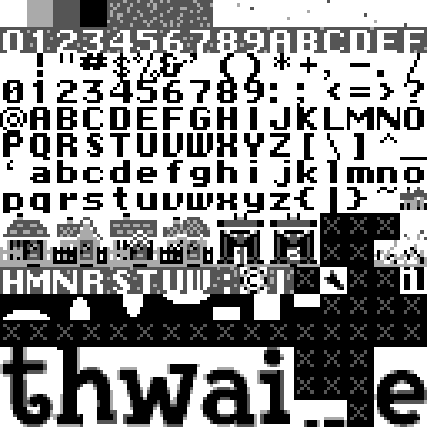
Pattern table0 ($4010-$500F):
Pattern table1 ($5010-$600F):
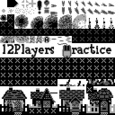
Keep in mind, each pattern table is displayed in a 16×16 tiles layout, left to right, top to bottom. But this is just to fit in the webpage width.
The tiles are actually stored as a "single strip", one after the other
Why is it in black and white?
Colors are not stored in pattern tables (why is explored at a later chapter).
Because of that, we rendered these in grayscale.
But even without the palette, we can discern the shapes: the font, the houses you defend, the missiles and explosion bursts, and the chunky title-screen letters spelling thwaite.
How is every tile represented in the data?
To teach how tiles are stored, I'll use the 1-tile little house
below the o and right to the ~ tiles from pattern table 0.
This is the house scaled up:

Notice how there's only 4 different grayscale tones, this will be important later.
We're gonna first obtain the 16 bytes of this tile and then we're going to convert them, somehow, into this image.
Getting the tile bytes address
To obtain those 16 bytes, we first need their address.
This tile is the tile 127 (0-based) counting left to right
(row 7, column 15 so 7*16 + 15 = 127).
And each tile takes 16 bytes, so 126*16=2032, in hex 0x7f0
Since the pattern table starts at 0x4010 + 0x7F0 = 0x4800
We can get the 16 bytes at 0x4800 with xxd:
> xxd -s 0x4800 -l 16 thwaite.nes
20 00 00 0a 7a fb ff 00 ┊ 24 2e ff f1 04 a5 a5 00
Rendering the image
The first 8 bytes of the tile are bitplane 0, and the latter 8 are bitplane 1. And we're going to show every byte in binary.
        bitplane 0 (low bit)         bitplane 1 (high bit)
row 0   $20  0 0 1 0 0 0 0 0      $24  0 0 1 0 0 1 0 0
row 1   $00  0 0 0 0 0 0 0 0      $2E  0 0 1 0 1 1 1 0
row 2   $00  0 0 0 0 0 0 0 0      $FF  1 1 1 1 1 1 1 1
row 3   $0A  0 0 0 0 1 0 1 0      $F1  1 1 1 1 0 0 0 1
row 4   $7A  0 1 1 1 1 0 1 0      $04  0 0 0 0 0 1 0 0
row 5   $FB  1 1 1 1 1 0 1 1      $A5  1 0 1 0 0 1 0 1
row 6   $FF  1 1 1 1 1 1 1 1      $A5  1 0 1 0 0 1 0 1
row 7   $00  0 0 0 0 0 0 0 0      $00  0 0 0 0 0 0 0 0
Now, merge both planes into a new grid. For each pixel, stack its high bit (plane 1) over its low bit (plane 0) to get a 2-bit number:
merged (high bit, low bit)
row 0   00 00 11 00 00 10 00 00
row 1   00 00 10 00 10 10 10 00
row 2   10 10 10 10 10 10 10 10
row 3   10 10 10 10 01 00 01 10
row 4   00 01 01 01 01 10 01 00
row 5   11 01 11 01 01 10 01 11
row 6   11 01 11 01 01 11 01 11
row 7   00 00 00 00 00 00 00 00
Now read each 2-bit number as a value 0–3:
0is transparent (shown as.to make the shape easier to see)1is light gray2is dark gray3is black
. . 3 . . 2 . .
. . 2 . 2 2 2 .
2 2 2 2 2 2 2 2
2 2 2 2 1 . 1 2
. 1 1 1 1 2 1 .
3 1 3 1 1 2 1 3
3 1 3 1 1 3 1 3
. . . . . . . .
Hopefully, via intuition, you'll see how every number matches the tile. And that's how the tiles are rendered from data.
But where's the color?
Color is determined from a selected palette, which is determined at runtime. We're gonna see that way later.
Checkpoint #1: Draw the graphics stored in a cartridge
You know what pattern tables are, where they live in the ROM, and how a tile's bytes turn into pixels. Now let's put a whole pattern table on screen.
The easiest way to do that is rendering it into an image file.
PPM, the easiest format
We need to write an actual image file, and the least painful one to produce by hand is PPM (portable pixmap, part of the Netpbm family alongside PGM for grayscale and PBM for black-and-white).
There's no library to pull in: a PPM is a tiny text header followed by pixel
values. The ASCII variant (P3) looks like this:
P3
4 2
255
255 0 0   0 255 0   0 0 255   255 255 255
0 0 0     0 0 0     0 0 0     0 0 0
P3— the magic, "ASCII color pixmap".4 2— width and height in pixels.255— the largest value a channel can take.- then one
R G Btriple per pixel, left to right, top to bottom.
That's a 4×2 image: a red, green, blue and white pixel on top, a black row
below. There's also P6, the same thing with the pixel data as raw bytes
instead of ASCII — smaller files, write that once the ASCII version works.
Notice how this format is just plaintext (not binary), and how 1 or more whitespaces are used as separators between the colors. That's why it's so friendly.
We're still in grayscale (color comes later), so map the four pixel values to four gray triples.
If RGB is new to you: each pixel is three numbers — red, green, blue — each from 0 to 255. When all three are equal you get a shade of gray, from
0 0 0(black) up to255 255 255(white).
So pick four evenly-spaced grays:
0→255 255 255(white)1→170 170 1702→85 85 853→0 0 0(black)
The goal, and the obstacle
We want the table laid out as a 16×16 grid of tiles, like the images in the previous chapter: 256 tiles, 8 pixels each, so a 128×128 image.
The obstacle is interleaving. PPM is written one full pixel row at a time, left to right, top to bottom. But tiles are stored as a strip, one complete tile after another. So the image's first pixel row isn't the first tile — it's row 0 of tile 0, then row 0 of tile 1, … up to row 0 of tile 15, then the image's second row is row 1 of those same 16 tiles, and so on. To emit the file in order you'd have to hop between 16 tiles per scanline. That bookkeeping is where it gets error-prone.
Build up to it
Don't fight the interleaving head-on. Add it last, one step at a time, so a bug has only one new thing it could be:
One tile. Render a single 8×8 tile to an 8×8 PPM. No layout problem at all — you're just checking your bitplane decode produces the right pixels.
A single column. Stack tiles vertically: an 8-wide,
8·N-tall image. This is the case worth noticing — when the image is one tile wide, a pixel row is a tile row, so writing the file in order is the same as walking the tiles in order. No interleaving yet, and you've confirmed you can place many tiles.More columns. Now go to the real grid. This is the step that introduces interleaving, and the clean way to handle it is to stop writing pixels straight to the file. Decode into an in-memory framebuffer — a flat
width × heightarray — and blit each tile into its(x, y)slot, then dump the whole buffer at the end. With random-access writes the strip-vs-grid mismatch disappears; serializing to PPM becomes a dumb loop that doesn't care how the pixels got there.
Doing it in this order means by the time you hit the grid, the only thing left to get wrong is the tile placement arithmetic — everything before it is already proven. It's slower to write but it makes the inevitable trial-and-error quick to pin down.
Blitting
Blit (short for bit block transfer, also written blitting) is the move in that last step: copy a small rectangle of pixels into a bigger buffer at some position. One tile is one blit.
Drawing the whole image is just that, in a loop — stamp each tile into its slot until the framebuffer is full:

Nothing special happens between tiles. Each blit writes its own 8×8 block and the next one writes the block beside it. Here's a single blit on its own, with the destination slot it lands in outlined:

The source can be any rectangle and you choose where it goes — copying one image into another at a position is a basic move you'll reach for constantly, not just here.
Milestone #2: Basic CPU
Before this one: from here on we're imitating the hardware, not yet understanding it. If that framing bothers you, I wrote about why it has to be this way in Imitate first, understand later.
The second milestone is a working 6502 CPU — the processor at the centre of the NES.
What it takes
- The CPU memory map — where the CPU reads and writes, so an instruction can actually fetch and store.
- The 6502 instruction set — the opcodes, their addressing modes, and the flags they touch.
- Checkpoint — the fetch–decode–execute loop and the state-logging that
lets you diff against
nestest.log.
CPU Introduction
The NES CPU is a Ricoh 2A03 — a 6502 with no decimal mode. Each cycle below is one memory access on the bus; the CPU never sits idle, so even "do nothing" steps show up as discarded reads.
CPU flow
The CPU is built to execute instructions sequentially, one by one, by reading them from memory. An instruction is 1, 2, or 3 bytes long, and the first byte is always the opcode ("operation code") — a one-byte number that identifies the instruction.
Addresses on this CPU are 16 bits long (2 bytes) — that's a 64 KiB
address space, $0000 to $FFFF.
The CPU tracks where it's reading from with a 16-bit register
called PC (program counter): the address of the next byte to read.
The basic operation read [PC]; PC++ is called a fetch. Executing an instruction is
a sequence of fetches — first the opcode, then the remaining bytes
(if any).
Cycle 1 of every instruction is therefore the same: fetch the opcode to identify the instruction.
So the whole CPU is a loop: fetch an opcode, do whatever it says, repeat.
loop {
    opcode = read(PC); PC++   // cycle 1: fetch the opcode
    execute(opcode)           // the rest of the cycles depend on the instruction
}
execute is empty for now — filling it in, one opcode at a time, is the work of
the checkpoint. Everything else on the CPU pages is
detail that hangs off this loop.
Example
Say PC = $8000 and memory contains:
$8000   C9
$8001   42
$8002   ...
The CPU is about to start a new instruction. It fetches the opcode:
cycle 1 read [$8000] → C9 (opcode); PC = $8001
C9 is the opcode for an instruction that does something specific
with one operand byte (what exactly isn't important here). The CPU
fetches the operand:
cycle 2 read [$8001] → 42 (operand); PC = $8002
PC sits at $8002, ready for the next opcode fetch.
CPU State
Below is a list of parts of the CPU that hold a value in execution, The reader needs to include these into whatever class that represents the CPU.
(If your programming language requires defining as signed or unsigned, use unsigned)
A (accumulator, 8 bits) — main scratch register; target of most ALU operations.
X, Y (8 bits each) — index registers; used by indexed addressing modes and as loop counters.
PC (program counter, 16 bits) — address of the next byte to read. Split into PCL (low 8 bits) and PCH (high 8 bits); the cycle breakdowns refer to them separately when the CPU updates one half without the other.
SP (stack pointer, 8 bits) — low byte of the stack address. The stack
lives in page 1, so the full address is 01:SP. Push decrements SP, pull
increments it.
P (status register, 8 bits) — the flags:
bit 7 6 5 4 3 2 1 0
    N V - B D I Z C
N (negative), V (overflow), B (break — only meaningful in the stacked copy pushed by PHP/BRK), D (decimal — ignored by the 2A03), I (interrupt disable), Z (zero), C (carry).
IR (instruction register, 8 bits) — holds the opcode of the instruction currently executing. Loaded at cycle 1.
AD (effective address latch, 16 bits) — where the current instruction's
operand address is assembled during addressing. Split into ADL (low) and
ADH (high). The lo and hi you'll see in the mode breakdowns are ADL
and ADH being written and later read as [ADH:ADL].
DL (data latch, 8 bits) — holds the most recent byte read from the bus; used to carry values between cycles.
"Fake" latches
The following latches exist in some form in the real hardware but are oversimplified here — though enough for accurate emulation. Include them too.
CL (carry latch, 1 bit) — remembers the page-crossing carry bit between the cycle that adds an index to the low address byte and the cycle that does the fixed-address re-read.
NEGATIVE (sign latch, 1 bit) — remembers the sign of a value across cycles, mainly for relative branches whose offset is negative.
IAL (intermediate ALU latch, 8 bits) — parks an ALU result between cycles so the next bus transaction can consume it.
Checkpoint #2: Match nestest
The 6502 has a lot of opcodes, and writing them all before running anything is a
long stretch with no feedback. nestest removes that. You make your emulator
print its state in the same format, run it alongside the log, and stop at the
first line that doesn't match — that line points straight at the bug.
So you build the CPU incrementally: implement an opcode, see how much further you get before the next mismatch, implement the one it tripped on, repeat. You're never debugging more than one instruction at a time.
The trap with a CPU is reading the whole instruction set before running
anything. Don't. The point of nestest is that the failing log is the
to-do list: it tells you which opcode to write next, one at a time. So we build
the smallest CPU that runs, point it at nestest, and let it tell us what's
missing.
The loop itself is small. Every opcode is unimplemented to start with:
loop {
    log_upcoming_instruction_and_state()
    opcode = read(PC); PC++
    switch (opcode) {
        // nothing here yet
        default: panic("unimplemented opcode {opcode:02X} at {PC-1:04X}")
    }
}
First rung: match line 1, with zero opcodes
nestest runs in automated mode: you force PC = $C000 at startup instead
of using the reset vector, and the rest of the state is the standard reset —
A=X=Y=00, P=24, SP=FD, and the cycle counter already at 7 (the reset
sequence burns seven cycles). So the first line of the log is:
C000 4C F5 C5 JMP $C5F5 A:00 X:00 Y:00 P:24 SP:FD CYC:7
(The 4C F5 C5 bytes and the JMP $C5F5 disassembly are a separate concern:
printing them means knowing each instruction's length, which only falls out once
you decode opcodes. Add those columns as you go, or leave them off the diff at
first — they're for humans, not for matching.)
The development loop
Run it against nestest.log and diff. With the skeleton, line 1's state
matches, then the CPU fetches 4C and panics: unimplemented opcode 4C. That's
your instruction:
- Look up
4Cin the instruction reference — it'sJMPabsolute. Implement just that one. - Rerun. The CPU now executes the jump, logs line 2, and panics on its opcode.
- Repeat. Implement the opcode it tripped on, see how much further you get.
You're never holding more than one instruction in your head. When the log stops
mismatching, you've matched nestest — and the CPU is the part you can now
trust.
CPU Instruction Guide
The full opcode table lives in the CPU Instruction Reference. This page explains how to read it.
Don't read it top to bottom because checkpoint #2 sends you there one opcode at a time.
There's 256 instructions, and they are identified by a onebyte opcode
(0x00 to 0xff). Each instruction has its own fixed behavior.
Most instructions are a unique pair of mnemonic, addressing mode:
Other instructions are mnemonic.
The opcode byte just encodes that pair. LDA $42
(opcode A5), zero page and LDA #$42 (opcode A9) are different instructions,
they have the same mnemonic (LDA), but different addressing modes.
The addressing mode describes how a specific value is obtained. The mnemonic usually describes what to do with that value.
Special instructions
There's a small group of unique instructions that don't have an addressing mode. They do unique work and I call these special:
JSR,RTS(subroutine call/return).BRK,RTI(interrupt entry/exit).PHA,PHP,PLA,PLP(stack push/pull).- The interrupt service sequence itself (not an instruction, but the
CPU runs a fixed cycle pattern on NMI/IRQ/RESET — it mirrors
BRK).
Operands
Instructions can have 0, 1 or 2 operands. The importance of this is just for matching nestest, because the format... (complete this)
Illegal instructions
Also known as undocumented instructions in official docs. Many (most?) games make use of these instructions, so they are included here. and the genuinely unstable ones carry a warning.
Flags
Flags are shown as N V - B D I Z C: a letter means the instruction sets
that bit, - means it's preserved. N and Z track the result — the
last value the instruction computes (the register it loads, the byte it
writes, or its final register update), which isn't always the output.
C and V, when touched, are spelled out in the entry.
Addressing modes
Addresses are written high:low when
assembled across cycles — typically ADH:ADL for the operand address
being built, or PCH:PCL for the program counter. Cycle 1 (opcode
fetch) is omitted from every mode below.
Access type. A memory mode doesn't pin down the cycles on its own: it works out where the operand is, but what happens at that address depends on the instruction's access type:
- read — fetch the operand from the address (
LDA,ADC,CMP, …). - write — store a register to the address (
STA,STX,STY). - read-modify-write (RMW) — read the operand, change it, write it back
(
INC,DEC,ASL,LSR,ROL,ROR).
Each instruction below is tagged with its access type. The memory modes share
their address-calculation cycles and then branch on it, shown as
Access type: read / write / rmw. Two things to notice in the branch:
- RMW writes twice — first the unmodified value (a dummy write the hardware
can't skip), then the modified one,
r. Each RMW instruction definesrin terms ofDL(e.g.ASL→r = DL << 1); see the instruction list. - Indexed writes and RMW don't get the page-cross shortcut. A read can finish a cycle early when the index stays on the page; write and RMW always pay the extra cycle, because they have to settle the address before touching it.
Implied, Accumulator, and Immediate have no memory operand to branch on, so
their single form is listed as-is — Accumulator is an RMW on A with no bus
access.
Opcodes in each group are listed ascending by value.
Dummy reads
Each cycle is written as assignments, Zig-style.
bus.read(addr) is a read bus cycle returning the byte at addr;
bus.write(addr, val) is a write cycle. _ = bus.read(addr) is a
dummy read: the CPU still drives the cycle on the bus, it just throws
the byte away (_ discards it, as in Zig). The hardware can't skip
these. // starts a comment.
Chip timing and the emulator loop
The NES has a few different chips — CPU, graphics (PPU), audio (APU) — and they all share a single source of time: a crystal oscillator on the board that sends out a pulse every ~47 nanoseconds. The stream of pulses it produces is called the master clock, and one pulse is one clock (or tick, or cycle).
Every chip is wired to the same pulse stream, but one cycle of work for each chip takes a different number of clocks to complete:
- PPU — one cycle every 4 clocks (~186 ns).
- CPU — one cycle every 12 clocks (~560 ns).
- APU — same as the CPU, 12 clocks. Some of its internal units run at half that rate (one cycle every 24 clocks).
The chips run at different cycle rates, but they are all in-sync to the same master clock.
Aside on vocabulary: in NES and 6502 documentation you'll see clock, tick and cycle sometimes used interchangeably to mean "one beat of some chip's clock." I prefer to use the terms "master clock" and "cpu cycle", "ppu cycle", but it's not a hard rule. Also, throughout these notes I count clocks and cycles starting at 1, not 0 — so the first clock of a CPU cycle is clock 1, the last is clock 12.
Coding the parallelism of chips
On the real console the chips run in parallel. In an emulator running on a modern CPU we can't reproduce that — using one thread per chip wouldn't make sense because the OS scheduler's has jitter, it can't be made to tick at exact intervals.
But we don't need real-time parallelism. What makes the emulation accurate is the order in which the chips tick in relation to each other.
There's two ways I noticed this can be coded:
- CPU-centric — the CPU drives, and the other chips are ticked from within its work.
- Master-clock centric — the master clock drives, and each chip ticks when its own divider says so. I barely mention this because I feel it's harder to implement
Chip Parallelism #1: CPU-centric
First, let's define what a CPU step is. It is one full CPU operation — either an instruction (2–7 cycles) or an interrupt service sequence (7 cycles). A CPU step is several CPU cycles long; a CPU cycle is 12 clocks.
Why multiple cycles per step? Because every read or write the
CPU does on the bus takes one full cycle, and an instruction is
defined as a sequence of bus accesses. LDA $1234 runs as:
- Read the opcode.
- Read the low byte of the address.
- Read the high byte of the address.
- Read the value at
$1234.
Four bus accesses, four cycles. The cycle count of an instruction is essentially "how many times it touches the bus."
A simple but incorrect first attempt:
while (true) {
    cycles = cpu.step();         // run one operation; returns # cycles (2–7)
    ppu.tick(cycles * 3);        // 3 PPU cycles per CPU cycle
    apu.tick(cycles);            // 1 APU cycle  per CPU cycle
}
The arithmetic is right — each chip gets the correct total amount of catch-up — but the order is wrong. The loop runs the CPU's entire step in one shot, then the PPU, then the APU. For a 2-cycle step it looks like this:
order of work:

     CPU:  ▓ ▓
     APU:      ▓ ▓
     PPU:          ▓ ▓ ▓ ▓ ▓ ▓
But, on the real console the three chips are running side by side, ticked off the same master clock. Each chip's cycle is a span of master clocks (12 for CPU and APU, 4 for PPU), and the spans overlap in time:
clocks:  0   4   8   12          24
   CPU:  ├───────────┼───────────┤    2 CPU cycles (12 clocks per cycle)
   APU:  ├───────────┼───────────┤    2 APU cycles (same as CPU)
   PPU:  ├───┼───┼───┼───┼───┼───┤    6 PPU cycles (4 clocks per cycle)
This is a good proof of concept of the interleaving we want.
Reproducing this interleaving is what emulation accuracy hinges on: the chips affect each other through the bus, and when a write or read lands relative to the other chips' progress changes what they observe. Not interleaving the order of chip ticks makes emulation diverge from real hardware.
To achieve this, every time the CPU does a
bus access (which is once per cycle), it should clock() 12 times
before moving on, because a CPU cycle takes 12 clocks:
fn cpu.step() {
    // ... while running the operation, for each cycle:
    bus.read(addr);              // bus.read internally calls tick_others()
}

fn bus.read(addr) {
    clock(12);
    const byte = read_byte(addr);
    return byte;
}

fn clock(n) {
    for (0..n) {
      master_clocks += 1;
      if (master_clocks % 4 == 0) ppu.tick(3);
      if (master_clocks % 12 == 0) apu.tick(1);
    }
}
Actually accurate cycle emulation
The former explanation was simpler for learning purposes, but for the emulation to be accurate the graph would be more like this:
clocks:     3   7   11  15  19  23
   PPU:  ───┼───┼───┼───┼───┼───┼─
   CPU:  ├────R──────┼──────W────┤
clocks:  0    5      12     19   24
              R = read (early, clock 5/12)
              W = write (late, clock 7/12)
We introduced two real hardware details here:
PPU/CPU phase offset. The PPU's ticks don't align with the
CPU's cycle boundaries — above they fire at clocks 3, 7, 11, …,
not 4, 8, 12, …. The offset is one of three values picked randomly
at power-on; I use -1. In clock function:
const ppu_offset = -1;
fn clock(n) {
  ...
  if ((master_clocks + ppu_offset) % 4 == 0) ppu.cycle();
  ...
}
Read vs write timing. The CPU's bus access lands at a specific master clock inside the 12-clock window with an offset altered by the current CPU cycle being a read or a write.
Above, cycle 1, which is a read, gets the value in clock 5, but cycle 2, which is a write, happens at clock 7 (late).
Reflected in bus.read / bus.write:
fn bus.read(addr) {
    clock(5);
    const byte = read_byte(addr);
    clock(7);
    return byte;
}

fn bus.write(addr, byte) {
    clock(7);
    write_byte(addr, byte);
    clock(5);
}
Aside: I'm not fully sure these are the "correct" splits — on real silicon both reads and writes happen during the second half of the cycle, and the exact master clock isn't fixed at a 1-clock granularity. The 5/7 and 7/5 numbers here are what Mesen uses for the common case, which is a reasonable starting point but not the final word.
Chip Parallelism #2: Master-clock centric
This way is worse for reasons specified further down.
The outer loop advances the master clock one clock at a time, and on each clock a switch decides which chips are due to step:
let clock = 0;
while (true) {
    clock += 1;
    if (clock % 4  == 0) ppu.cycle();
    if (clock % 12 == 0) cpu.cycle();
    if (clock % 12 == 0) apu.cycle();
}
Now each chip moves exactly when its divider fires, no chip ever runs ahead of another. That makes mid-cycle effects natural to express — a PPU event that happens on clock N+3 of a CPU cycle just happens, without the CPU loop having to know about it.
This has two challenges to implement:
1. The CPU has to be written as a state machine
In the master-clock-centric loop, cpu.cycle() is called once
per CPU cycle (every 12 clocks), but a full CPU instruction
takes 2–7 cycles. So a single instruction can't run top-to-
bottom in one call — it has to be sliced across as many calls as
the instruction has cycles, with the CPU itself remembering
where in the instruction it left off.
To see what this looks like in general: a straight-line function that does its work in one go looks like this:
fn cook_pizza() {
    knead_dough();
    add_toppings();
    bake();
}
If we can only do one step per call, the body has to become a switch on externalised state:
let stage = 0;

fn cook_pizza_step() {
    if      (stage == 0) knead_dough();
    else if (stage == 1) add_toppings();
    else if (stage == 2) bake();
    stage += 1;
}
Every NES instruction has to be written like this, with the
cycle index as the stage. The CPU-centric model avoids it —
instructions there stay as straight-line code.
This makes the code painful to write and slow at runtime: every
instruction grows a switch, and the outer loop now runs 12× per
CPU cycle instead of once.
2. Read/write timing inside a CPU cycle
Reads and writes land at different clocks within a CPU cycle, so
the boundary check has to shift by an offset that depends on
the access type of the next cycle. That means having a a per-
instruction, per-cycle table of "is read or write?" so the loop
has to know the right offset ahead of time:
while (true) {
    ...
    if ((clock + offset) % 12 == 0) cpu.cycle();
    ...
}
Again, annoying.
PPU
The PPU (Picture Processing Unit, the Ricoh 2C02) is the chip that draws the picture. The CPU never touches the screen directly — it talks to the PPU through eight memory-mapped registers, and everything the PPU does on its own (scrolling, fetching tiles, compositing sprites) runs off a second set of registers the CPU can't address at all.
So there are two register files, and it's worth keeping them apart: the CPU-visible ones the program reads and writes, and the internal ones that hold the rendering state.
CPU-visible registers
Memory-mapped at $2000–$2007 and mirrored every 8 bytes up through
$3FFF (so $2008 is $2000 again, and so on). The CPU only ever sees the
PPU's state through these.
PPUCTRL ($2000, write) — top-level configuration:
bit 7  NMI on vblank   (1 = fire an NMI when vblank begins)
bit 6  master/slave    (unused on the NES)
bit 5  sprite size      (0 = 8x8, 1 = 8x16)
bit 4  background pattern table  (0 = $0000, 1 = $1000)
bit 3  sprite pattern table      (0 = $0000, 1 = $1000, 8x8 only)
bit 2  VRAM increment   (0 = +1 across, 1 = +32 down) per PPUDATA access
bits 1-0  base nametable select  (also written into `t`)
PPUMASK ($2001, write) — what's switched on and how color is filtered:
bits 7-5  emphasize blue / green / red
bit 4  show sprites
bit 3  show background
bit 2  show sprites in the leftmost 8 pixels
bit 1  show background in the leftmost 8 pixels
bit 0  grayscale
Bits 3 and 4 are the master rendering switches; with both off the PPU emits only the backdrop and stops fetching.
PPUSTATUS ($2002, read) — three flags in the top bits:
bit 7  vblank started
bit 6  sprite 0 hit
bit 5  sprite overflow
bits 4-0  stale PPU bus contents (open bus)
Reading it has two side effects: it clears the vblank flag (bit 7) and
resets the write toggle w. That second effect is why the usual idiom
is to read $2002 before writing a scroll or address — it guarantees the
next double-write starts on its first half.
OAMADDR ($2003, write) — the index into
OAM (Object Attribute Memory, the 256-byte
sprite store) that OAMDATA reads or writes.
OAMDATA ($2004, read/write) — read or write the OAM byte at OAMADDR;
writing increments OAMADDR. Games rarely use this directly — OAMDMA is the
normal path.
PPUSCROLL ($2005, write twice) — the scroll position, two writes using
w: first write is the X scroll, second is the Y scroll. The values land in
t (and the fine-X bits in x), not in any register of their own.
PPUADDR ($2006, write twice) — the VRAM address for PPUDATA, two
writes using w: first the high 6 bits, then the low 8. It writes into t,
then copies t into v. Because it shares t with PPUSCROLL, scroll and
address writes step on each other — that overlap is a whole topic of its
own.
PPUDATA ($2007, read/write) — read or write VRAM at v, then
increment v by 1 or 32 (per PPUCTRL bit 2). Reads are buffered:
$2007 returns the previous read and refills the buffer behind it, so a
read of normal VRAM is one access stale (palette reads at $3F00+ are the
exception and come back immediately).
One more lives on the CPU's side of the bus, not the PPU's, but it's how OAM actually gets filled.
OAMDMA ($4014, write) — write a page number $XX and the CPU copies
all 256 bytes of $XX00–$XXFF into OAM in one go (513–514 cycles, the CPU
stalled throughout).
Internal registers
Not addressable. The CPU nudges these only through the registers above. This is where scrolling and the rendering pipeline actually live.
v (current VRAM address, 15 bits) — the address the PPU is fetching
from right now, advancing as it walks tiles across and down.
t (temporary VRAM address, 15 bits) — the staging copy, where
PPUSCROLL/PPUADDR writes accumulate; also describable as the address of the
top-left on-screen tile. Copied into v at fixed points (all of it on the
pre-render line, the horizontal bits at the start of each visible line).
v and t are the two loopy registers, named after the write-up that
first documented them. They're called "VRAM address" registers, but their
15 bits are laid out so the same value is the scroll position — which is
the trick that makes scrolling cheap (move the camera = change an address):
 yyy NN YYYYY XXXXX
 ||| || ||||| +++++-- coarse X    (tile column, 0-31)
 ||| || +++++-------- coarse Y    (tile row, 0-29)
 ||| ++-------------- nametable select (which of the four)
 +++----------------- fine Y      (pixel row within the tile, 0-7)
x (fine X scroll, 3 bits) — the sub-tile horizontal offset (fineX),
the part of the scroll that moves within a single tile.
w (write toggle, 1 bit) — first-or-second-write latch, shared by
PPUSCROLL and PPUADDR. Cleared by reading PPUSTATUS.
The rest of the internal state is the rendering pipeline — the registers that turn fetched bytes into pixels. The full mechanics live in their own chapters; here's what each one holds.
The PPUDATA read buffer (8 bits) — backs the one-access-stale read
described under PPUDATA: a $2007 read hands back this byte, then the
buffer reloads from v.
BG pattern shift registers (two, 16 bits each) — hold the
two bitplanes of the tile being drawn. Each is 16 bits rather than 8 because
the top half is the current tile and the bottom half is the next tile,
already fetched. The pixel emitted each dot is the bit at 15 - fineX, and
everything shifts left one place per dot — so over 8 dots a tile clocks out
and the next one slides up into place. See
the background pipeline.
BG attribute shift registers (two, 8 bits each) — carry the palette bits the same way: one value latched per tile and streamed alongside the pattern bits, so the palette stays in step with the pixels it colors.
The eight sprite units — the sprite-side equivalent, one per sprite chosen for the line. Each holds a pair of 8-bit pattern shift registers, an attribute latch, and an X-position counter that ticks down to the sprite's column before the unit starts shifting out its 8 pixels. Loaded from secondary OAM. See sprite evaluation and the priority mux.
Rendering Background
The background (also called the backdrop or playfield) is the scrolling world behind the sprites — the bricks, pipes and sky in Super Mario Bros. By the end of this chapter it's on screen, in color, and moving as the game scrolls.
Three steps:
- Static dump — the SMB title screen, grayscale. A warm-up that gets pixels up fast and gives us a known-good image to check against.
- The rendering pipeline — draw it the way the console does, one pixel per dot, fetching tiles as the beam sweeps. This is the bulk of the chapter, and it's what makes the screen scroll. Still grayscale.
- Color — feed the palette in.
Color comes last because it's a leaf you bolt on at the end — steps 1 and 2 stay
in grayscale. We take for granted that the PPU's eight registers
($2000–$2007) already read and write correctly, so VRAM holds the right
nametable and the pattern tables
hold the right tiles.
Step 1 — Static dump
A nametable is a 32×30 grid of tile indices; a pattern table turns each index into an 8×8 tile of 2-bit pixels. That's a whole screen, so draw it the dumb way: at the end of a frame, walk the 960 tile bytes, decode each tile, blit it into a 256×240 framebuffer.
for row in 0..30:
    for col in 0..32:
        let tile = nametable[row * 32 + col]
        let pixels = decode_tile(bg_pattern_table, tile)
        blit(framebuffer, pixels, col * 8, row * 8)
show(framebuffer)
This is the milestone-1 blit, with a nametable as the
source instead of the raw pattern table. bg_pattern_table comes from PPUCTRL bit
4 ($0000 or $1000). Map the four pixel values to four grays — 0→white,
3→black:
3 3 3 3 3 3 3 3
1 1 1 1 1 1 1 3
2 2 2 2 2 2 2 3
2 1 2 1 2 1 1 3
2 2 1 2 1 1 1 3
2 1 2 1 2 1 1 3
2 2 1 2 1 1 1 3
2 1 2 1 2 1 1 3
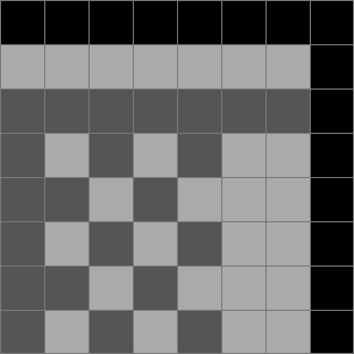
On the background, value 0 is not transparent the way it is for a sprite —
it's the backdrop color, the sky. For now it's just another gray; in step 3 it
becomes the universal background color.
Point this at Super Mario Bros. on its title screen and you should read "SUPER MARIO BROS." in gray — nametable 0 through pattern table 1. If it's garbled, stop: the problem is in the data or the decode, before any of the machinery below.
Step 2 — The rendering pipeline
The static dump can't scroll and isn't how the console works. The PPU draws one pixel per dot (one PPU clock; 341 per scanline) and never holds the whole nametable — it fetches a couple of bytes just ahead of the beam, clocks them out through shift registers, and walks the fetch address as it goes. That walk is the scroll: get it right and the screen moves for free.
Coarse and fine
Almost everything here is about naming a pixel, and the PPU splits that into two parts per axis: which tile, and which pixel inside the tile — the coarse and fine halves.
- coarse X / coarse Y — the tile's cell in the 32×30 nametable grid (X 0–31, Y 0–29).
- fine X / fine Y — the offset inside that tile, 0–7 each.
A pixel's position on each axis is coarse * 8 + fine. Scrolling by whole tiles
moves the coarse part; scrolling by a few pixels moves the fine part.
One asymmetry that explains a lot of the later code: fine Y lives inside v,
but fine X is its own register, x. Fine Y changes which bytes you fetch — a
tile's pattern is stored one byte per row, so the read address has to include it.
Fine X changes nothing about the fetch; it only picks which bit of an
already-fetched byte comes out. So fine Y rides in the address, while fine X is
held back and applied at the very end, as a pixel leaves the shift register.
The registers
The pipeline is short: VRAM → one latch per fetched byte → a shift register that
clocks a bit out per dot → a pixel. The address registers v/t/x are the
loopy registers from the PPU chapter; the latches and shift
registers are new here.
v  15b  current VRAM address — read pointer and scroll
t  15b  staging copy; PPUSCROLL writes it, copied into v
x   3b  fine-X; picks which bit of a tile is output

  fetch latch                shift register (1 bit/dot out)
  ─────────────────────      ──────────────────────────────
  nt_latch   tile index      (none; only addresses pattern)
  bg_lo_latch  plane 0    →  bg_pattern_lo  16b ┐ 2 tiles
  bg_hi_latch  plane 1    →  bg_pattern_hi  16b ┘ in flight
  at_latch   attr byte    →  bg_attr_lo      8b ┐ current
                             bg_attr_hi      8b ┘ tile
The attribute byte covers a 4×4-tile block. The 2 bits for this tile's quadrant
get parked in bg_attr_latch (2 bits) and fed into bg_attr_lo/hi one bit per
dot — more on that at the boundary below.
The scanline
Each visible scanline (0–239) spends its 341 dots like this:
dots 0       idle
dots 1-256   draw the 32 visible tiles (8 dots each)
dots 257-320 sprite fetches — background idle
dots 321-336 prefetch the next line's first 2 tiles
dots 337-340 dummy fetches
Sprites are a later chapter, so ignore 257–320 for now. The pre-render line (261) runs the same fetches but draws nothing, priming the registers for line 0.
The 8-dot tile cycle
A tile is 8 pixels wide, so it gets 8 dots, and two things run in parallel the
whole time. The shift registers clock pixels out — from a tile fetched
earlier — while four two-dot reads pull a later tile's bytes in. At dot 8 the
fetched tile drops into the registers and v steps one tile right.
The four reads. Every address comes from v, whose 15 bits are
yyy NN YYYYY XXXXX — fine-Y / nametable / coarse-Y / coarse-X:
nt_addr = 0x2000 | (v & 0x0FFF)
at_addr = 0x23C0 | (v & 0x0C00)
                | ((v >> 4) & 0x38) | ((v >> 2) & 0x07)
bg_addr = (bg_pattern_table << 12) | (nt_latch << 4) | ((v >> 12) & 7)
dots 1-2:  nt_latch    = ppu_read(nt_addr)
dots 3-4:  at_latch    = ppu_read(at_addr)
dots 5-6:  bg_lo_latch = ppu_read(bg_addr)
dots 7-8:  bg_hi_latch = ppu_read(bg_addr + 8)
bg_addr is the low bitplane, bg_addr + 8 the high
one — and both are built from nt_latch. That dependency fixes the order: you
can't address the pattern until the nametable read says which tile it is, so NT
comes first and the pattern bytes last. The attribute byte holds four quadrants'
palettes; coarse X/Y pick this tile's 2-bit one:
quad_shift = ((v >> 4) & 4) | (v & 2)
palette    = (at_latch >> quad_shift) & 3
Where the bytes go. The pattern registers are 16 bits and hold two tiles: the high byte is the tile being drawn, the low byte the next one, already fetched. Fine-X selects the output bit, which is how a scroll part-way into a tile works:
fine-X picks the output bit:  bit = (reg >> (15 - x)) & 1

  15 .......... 8   7 .......... 0    ◄ shift left 1/dot
  └ current tile ┘  └─ next tile ─┘
That two-tile lead is why dots 321–336 of the previous line had to prefetch: at dot 1 of this line the registers are already primed.
The boundary (dot 8). The four latches reload the registers' low bytes, and
the quadrant's palette bits go into bg_attr_latch:
bg_pattern_lo = (bg_pattern_lo & 0xFF00) | bg_lo_latch
bg_pattern_hi = (bg_pattern_hi & 0xFF00) | bg_hi_latch
bg_attr_latch = palette
Emit, every dot. On dots 1–256, read the top bit of each register for the
pixel, then shift them all left — the attr registers taking a fresh bit from
bg_attr_latch:
bit0 = (bg_pattern_lo >> (15 - x)) & 1
bit1 = (bg_pattern_hi >> (15 - x)) & 1
pal0 = (bg_attr_lo    >> (7 - x)) & 1
pal1 = (bg_attr_hi    >> (7 - x)) & 1
value   = (bit1 << 1) | bit0
palette = (pal1 << 1) | pal0
framebuffer[scanline][dot - 1] = gray[value]

bg_pattern_lo <<= 1
bg_pattern_hi <<= 1
bg_attr_lo = (bg_attr_lo << 1) | (bg_attr_latch & 1)
bg_attr_hi = (bg_attr_hi << 1) | (bg_attr_latch >> 1)
Grayscale ignores palette for now — step 3 reads it instead of throwing it
away. Here's a row coming out, real SMB pixels as fat blocks, the tile boundaries
every 8 dots:

And the same row with x = 3 — the bit selection starts three pixels into the
tile, so the whole row slides left, boundaries and all:

Scrolling — walking v
Nothing above moved the camera; v only has to advance correctly, and because
it's both the read pointer and the scroll position, that advance is the scroll.
Four updates, at fixed points in the line:
Every 8 dots — increment X. Step one tile right; at coarse X 31, wrap to 0 and flip the horizontal nametable bit so the walk continues into the next screen:
if (v & 0x001F) == 31:     # coarse X at the last column
    v &= ~0x001F           # wrap it to 0
    v ^= 0x0400            # flip horizontal nametable
else:
    v += 1
At dot 256 — increment Y. Step one pixel row down: bump fine Y, carry into coarse Y, flip the vertical nametable at row 29.
At dot 257, and again on the pre-render line — reload from t. By now v has
walked off to the right and down, so it's restored from t, the staging copy
PPUSCROLL writes — the horizontal bits every line, the vertical bits once per
frame:
dot 257:       v = (v & ~0x041F) | (t & 0x041F)   # X
dots 280-304:  v = (v & ~0x7BE0) | (t & 0x7BE0)   # Y, pre-render only
These reloads are the only path from the scroll the game wrote into v, so this
is where scrolling actually happens. Pin v = t = $2000, x = 0 and you get
step 1's title screen back exactly; let PPUSCROLL move them and SMB's overworld
scrolls as Mario walks, straddling two nametables (SMB uses vertical mirroring).
Still grayscale — the only thing that can be wrong here is the address math.
Step 3 — Color
Every pixel already arrives with a 4-bit index: palette (2 bits) and value (2
bits). Turn it into a palette-memory address:
let addr = 0x3F00 | (palette << 2) | value
$3F00–$3F1F is palette RAM (the palette table): eight 4-color palettes,
the low half for the background. Value 0 is the catch — every palette's entry 0
mirrors $3F00, the universal backdrop, the one color behind everything (the
sky). That's why background value 0 wasn't transparent in step 1:
if value == 0:
    addr = 0x3F00
let nes_color = palette_ram[addr & 0x1F] & 0x3F
That's a 6-bit number, 0–63: an index into the master palette (the system
palette), the 2C02's fixed 64-color RGB table. One more lookup and the grayscale
write from step 2 becomes a real pixel:
framebuffer[scanline][dot - 1] = MASTER_PALETTE[nes_color]
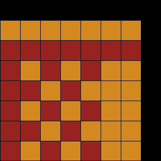
The result is blocky color regions: the palette comes from the attribute table, where every 2×2 tiles share one entry, so color is assigned in 16×16-pixel patches. Here's the step-1 tile in gray, then the same tile once its index runs through the two lookups:
What's left
The background is on screen, colored and scrolling. The remaining background details don't change the picture much:
- PPUMASK's grayscale bit (forces every color through
& 0x30) and the three emphasis bits that tint the output. - The leftmost-8-pixels clip, also in PPUMASK.
- The two dummy nametable fetches at dots 337–340, and the single dot skipped on odd frames when rendering is on.
The next thing that does change the picture is sprites, which ride on top of all this — and where the mid-frame scroll split (a fixed status bar over a moving level) finally gets driven, by sprite-0 hit.